
ETH researchers have built an ultrafast chip that can speed up data transmission in fibre optic networks. The chip combines several innovations at the same time and, given the growing demand for streaming and online services, represents a significant development.
Researchers from ETH Zurich have achieved what scientists have been attempting to do for some 20 years: in their laboratory work as part of European Horizon 2020 research projects, they have manufactured a chip on which fast electronic signals can be converted directly into ultrafast light signals – with practically no loss of signal quality. This represents a significant breakthrough in terms of the efficiency of optical communication infrastructures that use light to transmit data, such as fibre optic networks.
In cities like Zurich, these fibre optic networks are already being used to deliver high-speed internet, digital telephony, TV, and network-based video or audio services (“streaming”). However, by the end of this decade, even these optical communication networks may reach their limits when it comes to rapid data transmission.
This is due to the growing demand for online services for streaming, storage and computation, as well as the advent of artificial intelligence and 5G networks. Today’s optical networks achieve data transmission rates in the region of gigabits per second. In the future, however, transmission rates will need to reach the terabit region.
The key to this paradigm shift lies in combining electronic and photonic elements on a single chip. The field of photonics studies optical technologies for the transmission, storage and processing of information.
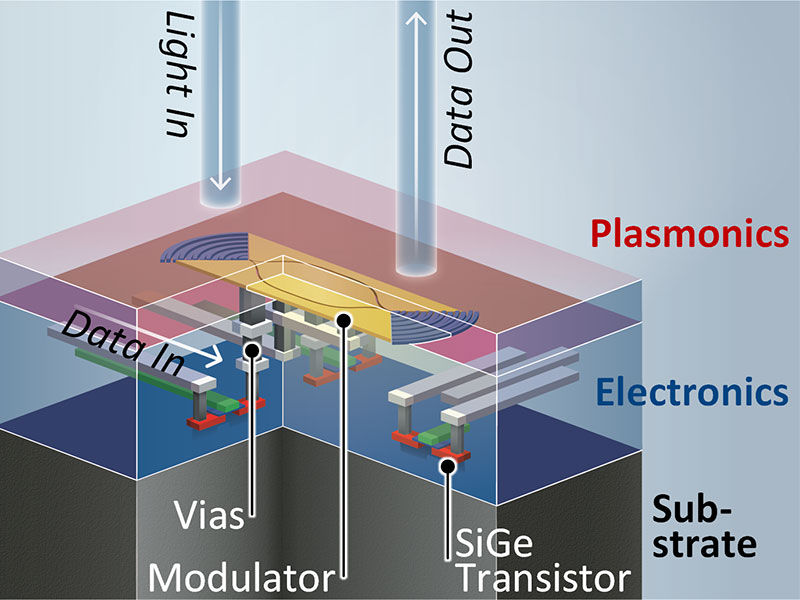
The ETH researchers have now achieved precisely this combination: in an experiment performed in collaboration with partners in Germany, the US, Israel and Greece, they were able to bring together electronic and light-based elements on one and the same chip for the first time. This is a huge step from a technical perspective, because these elements currently have to be manufactured on separate chips and then connected up with wires.
There are consequences to this approach: on the one hand, manufacturing the electronic and photonic chips separately is expensive. On the other hand, it hampers performance during the conversion of electronic signals into light signals and thereby limits the transmission speed in fibre optic communication networks.
The research team’s approach therefore begins with the modulator, a component on the chip that generates light of a given intensity by converting the electrical signals into light waves. The size of the modulator must be as small as possible in order to avoid a loss of quality and intensity in the conversion process, and in order to transmit the light – or rather the data – faster than is possible today.
This compactness is achieved by placing the electronic and photonic components tightly on top of one another, like two layers, and connecting them directly to the chip by means of “on-chip vias”. This layering of the electronics and photonics shortens transmission paths and reduces losses in terms of signal quality. As the electronics and photonics are implemented on one single substrate, the researchers describe this approach as “monolithic co-integration”.
For the past 20 years, the monolithic approach has failed because photonic chips are much bigger than electronic ones. This prevented them from being combined on a single chip. The size of the photonic elements makes it impossible to combine them with the metal oxide semiconductor (CMOS) technology that is prevalent in electronics today.
The researchers have now overcome the size difference between photonics and electronics by replacing the photonics with plasmonics.
Plasmonics can be used to squeeze light waves into structures that are much smaller than the wavelength of the light.
As the plasmonic chips are smaller than electronic ones, it is now actually possible to manufacture much more compact, monolithic chips that incorporate both a photonic and an electronic layer. In order to then convert the electrical signals into even faster optical ones, the photonic layer contains a plasmonic intensity modulator. This is based on metal structures that channel the light in order to reach higher speeds.
This is in addition to a speed increase in the electronic layer. In a process known as “4:1 multiplexing”, four lower-speed input signals are bundled and amplified so that, together, they form a high-speed electrical signal. This is then converted into a high-speed optical signal. In this way, the researchers were able to transmit data on a monolithic chip at a speed of over 100 gigabits per second for the first time.
News Source: ETH
